An Accidental Discovery
Most physical items are made of 3D materials. Solid materials are often made of either organized atoms in per-determined 3D structures forming metals and crystals or disorganized atoms forming other things.
For a long time, this was assumed to be the only form in which matter could be organized to form solid objects. But 20 years ago (2004), two researchers at the University of Manchester, Andre Geim and Professor Kostya Novoselov, discovered a 2D material, graphene. They discovered it almost by accident when they realized that simple scotch tape applied of graphite ( what makes pencil tips) created a mono-atomic layer of carbon.
This would later win them the 2010 Nobel Prize in Physics.
Graphene is made of carbon atoms, but instead of being in disorganized form (graphite) or organized crystal (diamonds), in graphene, the carbon atoms are aligned in a mono-atomic layer, like an ultra-thin paper sheet. They also discovered that it is even possible to form 1 or zero-dimension materials, like nanotubes or quantum dots.
Source: Ossila
What makes 2D materials special is that this unique configuration comes with unique physical properties.
For example, graphene is extremely conductive, with electrons able to circulate in it at 1/300th the speed of light. It is also a very good thermal conductor and has the highest tensile strength of any material despite being optically transparent, absorbing only 2% of incident visible light.

Source: Visual Capitalist
So Much More Than Graphene
Graphene’s unique properties immediately made it the focus of thousands of researchers eager to unveil its unique electrical, chemical, and physical properties.
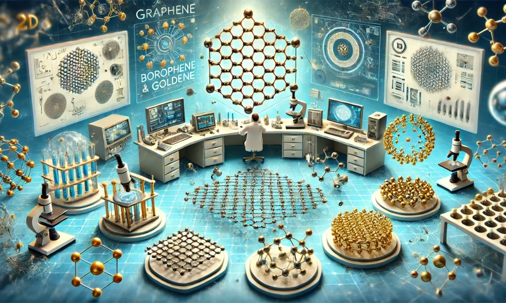
However, others started to wonder if other elements other than carbon could create 2D materials as well. The answer was yes, with theoretical prediction promising hundreds of different potential 2D materials. Among the most important and studied 2D materials besides graphene, we can mention a few:
- Borophene, made of boron atoms, discovered only in 2015.
- Goldene, made of gold atoms, produced first in 2024.
- Silicene, made of silicon atoms.
- Phosphorene, made of phosphorus atoms.
It also appears that 2D materials do not have to be made of only one pure element—for example, mono-layers of molybdenum disulfide (MoS2) or silicon nitride (Si3N4).
Other atoms can also be attached to the monolayer, creating a “rugged” surface, like when adding hydrogen to the carbon atoms of graphene to form graphane.

By Edgar181 (talk) – Own work, Public Domain, https://commons.wikimedia.org/w/index.php?curid=12091234
Because of this extreme diversity of material, researchers are only beginning to uncover the potential of 2D materials.
Applications – Fundamental Aspects
In general, what makes 2D materials unique is that their very organized atomic structure allows for the unique configuration of their electrons and the tight bond between the atoms.
This in turn explains the exceptional electrical conductivity (flow of electrons), thermal conduction (transfer of the energy levels between atoms), and physical strength (covalent bonds between atoms due to exchanging electrons).
The 2D structure also gives these materials the highest specific surface areas (surface where interactions are possible) of all known materials. This makes them excellent candidates for new forms of catalysts or, in general, getting involved in chemical and electrical reactions.
Superconductors
Because electrons flow almost entirely freely at the surface of 2D materials, they have been considered good candidates for superconductivity.
Superconductivity is what happens when a material is able to conduct electricity without any resistance.
This means that not only is there no energy loss, which could be very useful for carrying power over long distances, but it also means that a current passing through the material does not generate any heat. This can make it incredibly useful for all sorts of applications, from computing to EVs and virtually any technology that uses electricity.
In theory, superconductivity, especially room-temperature superconductivity could allow for mastering nuclear fusion, propelling ships with electricity, cheap & ultra-fast maglev trains, mass drivers to reach orbit at a very low cost, etc. (We explored in further detail the question of room-temperature superconductors in our dedicated article).
Plenty of 2D materials might display superconductivity in the right conditions (e.g., temperature, pressure, etc.,) including:
- Elemental metal ultrathin films.
- Cuprates.
- Perovskite oxides.
- Rare-earth metal heavy-fermion compounds.
- Graphene.
- Iron selenide on oxide surfaces.
- Organic conductors on metal surfaces.
Semiconductors
Semiconductors are materials able to selectively switch from a conductive state (which transfers electrons) to an isolant state (which blocks electrons). This is the fundamental principle around which silicon transistors and other computing elements are built, with 0 being no electric current and 1 the presence of current.
The quickest a semiconductor can change state, the quicker the associated computation can be.
Graphene
At first, researchers studying graphene thought it could replace silicon in semiconductors. Unfortunately, it misses a key electronic feature called a “band gap.”
A band gap is what determines if a material will be considered a metal (conducting electricity), an isolator (blocking electricity), or a semiconductor (that can switch between being conductive and isolant).

Source: Energy Education
The problem is that graphene has no band gap at all, preventing its use as a semiconductor.
This was true until 2024 when researchers announced they managed to create the world’s first semiconductor made of graphene.
“We now have an extremely robust graphene semiconductor with ten times the mobility of silicon, and which also has unique properties not available in silicon.
“We had to learn how to treat the material, how to make it better and better, and finally, how to measure the properties. That took a very, very long time.”
Goldene
Another 2D material of interest is goldene, essentially graphene but with gold replacing the carbon atoms.
Gold is already commonly used in chips and computer components thanks to its extraordinary properties, like resistance to oxidation and very high electrical conductivity.
With the production in 2024 of the first goldene monolayer, semiconductor properties might be added to the list.
“If you make a material extremely thin, something extraordinary happens – as with graphene. The same thing happens with gold. As you know, gold is usually a metal, but if a
layer is a single atom thick, then gold can become a semiconductor instead.”
Organic Semiconductors
Organic molecules are made of a skeleton of carbon, together with other elements, commonly oxygen, nitrogen, sulfur, etc.
Recently, researchers discovered that they can force organic polymers to stay in 2D configuration and avoid multiple layers stacking on each other.

Source: POSTECH
They then used a step called p-type doping, commonly used in the production of semiconductors.
This refers to adding elements to a semiconductor material to make it even more conductive.

Source: Wikipedia by VectorVoyager
The resulting material has been described by the researchers as having “outstanding electrical conductivity”.
So even if somehow materials like graphene are too difficult to mass produce in a semiconductor configuration, or goldene is too expensive, organic semiconductors will probably be there to allow the adoption of 2D semiconductors in the near future.
Super-Materials
While electrical properties are the core of scientists’ interest in 2D materials, their physical properties are equally impressive.
For example, graphene is 200x times stronger than steel for an equivalent mass. Graphene could be integrated into concrete, the way steel is in armored concrete, creating a concrete 2.5x stronger and 4x less water permeable. In addition, graphene does not rust like steel, making graphene-reinforced concrete not vulnerable to “concrete rot” caused by iron oxidation, which severely limits the lifespan of concrete structures.

By Achim Hering – Own work, CC BY 3.0, https://commons.wikimedia.org/w/index.php?curid=20269527
The extreme resistance + light weight of graphene and other 2 materials could also be used to create better body armor.
Another field of application can be thermal management. For example, researchers found recently that you can manufacture a material that is both isolant and stiff (a rare combination) by creating 2D hybrid organic-inorganic perovskites.
2D materials like graphene and hexagonal boron-nitride could also be used to dissipate heat in electronic and optoelectronic devices.
Lastly, advanced ultra-resistant 2D materials could be used to achieve futuristic infrastructures, like for example space elevators. However, such steps will only be realistic once we have figured out how to economically produce these materials not by the grams or kilos, but by the millions of tons.
Biotech
Very high surface level, extremely thin layer, and unique chemical properties make 2D materials good candidates for plenty of niche applications in the medical and biotech industries.
This includes drug delivery, imaging, tissue engineering, biosensors, and gas sensors.
Another factor in the emergence of 2D materials in biological applications is the recent discoveries allowing them to give them a characteristic called chirality.
Chirality is a chemistry term that means that molecules have a left/right symmetry. Chirality is an important feature of organic molecules, for example, the amino acids that are the building blocks of proteins.

Source: UC Santa Barbara
In molecules, chirality can make biological or chemical units exist in two versions that cannot be perfectly matched, as in a left and right mitten. They can mirror each other precisely, but a left mitten will never fit the right hand as well as it fits the left hand.
Pr. Dipanjan Pan
Recently, researchers synthesized borophene platelets, similar to how fragments of borophene would go into the bloodstream. They discovered that the chiral properties of the different versions of borophene interacted differently with the cells’ membranes, and entered the cells differently.
This opens the way to designing custom borophene structures for applications like the “development of higher-resolution medical imaging with contrast that could precisely track cell interactions or better drug delivery with pinpointed material-cell interactions.”
A better understanding of how borophene structure interacts with living cells will also help clarify its safety profile.
While borophene’s health profile is still being evaluated, it appears that graphene can even be safely inhaled without any acute risk to human health. These results are still very preliminary but likely indicate that the quick proliferation of 2D materials should not result in public health issues.
And the more bio-compatible they are, the more likely they can be used to develop biological sensors or power nanorobots in our bloodstream.
Limitations
Manufacturing At Scale
Even the most established and first discovered 2d material, graphene, is still very much the domain of laboratories and startups.
This is because producing it at scale is still a tricky proposition. Making small amounts is sort of easy, but producing massive amounts in a semi-automatized way is not.
Scotch tape applied to a piece of graphite was enough to discover graphene. But much more complex methods like Chemical Vapor Deposition (CVD) are required for mass production.
This is slowly becoming more of a reality, with, for example, the publication of a process for oxygen-free CVD producing high-purity graphene.
Gluing It
Another issue with 2D materials is that because they are so thin and unique chemically, they can be difficult to glue onto other materials.
It often requires specialized techniques to get a layer of graphene to stick to computer chips, a power supply, or a medical device.
This can be a lot more time-consuming and resource-intensive than less efficient but easier-to-implement alternatives.
Costs
Because for now, most production methods and applications to existing devices are mostly small-scale or bespoke, 2D materials have stayed rather expensive.
Actual price can greatly vary depending on purity, with for example graphene ranging between $20-2,000/kg.
This means that even at the cheapest price, graphene is still 20x more expensive than steel. In addition, to achieve acceptable performance in replacing said steel, probably more than the lowest possible purity is required.
2D Material Companies
The field of 2D materials is evolving very quickly, with new options like goldene being discovered regularly, and new insight into how to optimize “old” materials like turning graphene into a semiconductor.
These products will likely only become a major economic sector once produced at scale using industrial methods.
So far, the most advanced and well-documented method is CVD, giving a significant advantage to CVD specialists to capture a lot of the value of 2D materials manufacturing.
1. Veeco
Veeco has been a major supplier of equipment to the semiconductor manufacturing industry since its foundation in 1945. Its machines are used in producing advanced EUV chip making, 5G antennas, hard drives, LIDAR, LEDs, power electronics for EVs, etc.

Source: Veeco
The company’s main technological focus is the same CVD process used for borophene production, or more precisely, MOCVD (Metal-Organic Chemical Vapour Deposition).

Source: Veeco
As a leader in this niche segment of the semiconductors industry, Veeco could be a good candidate to bet on the rise of more CVD applications.
Such growth could be stemming from the growing usage of graphene, tungsten, and borophene, as we progressively get better at manipulating matter at the atomic level.
It will also likely benefit from the massive trends of digitalization, AI, and electrification, whether it massively uses 2D materials soon or not.
2. Graphene Manufacturing Group (GMG)
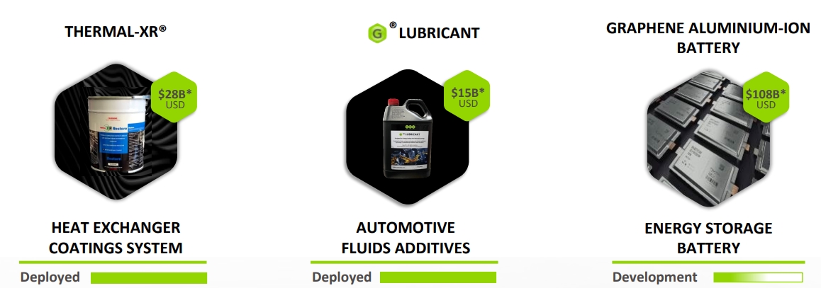
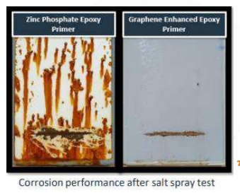
GMG is a graphene producer that has focused its product offering on already demonstrated graphene-based products like heat coating and lubricants.
This makes GMG a good option for investors looking for direct exposure to the graphene market and a company already active in mass-producing graphene and improving the current production method.

Source: GMG
Some further applications could be the creation of graphene semiconductors (see “Graphene Semiconductors – Are They Finally Here?”), or even room-temperature superconductors. Graphene coating could also find use in batteries and for hydrogen pressure vessel technologies.

Source: GMG
GMG produces its graphene from methane + hydrogen, which differs from most of its competitors, who produce it from graphite natural deposits. This allows for higher purity, more scalability, and low-cost production.
The company launched its first production facility in Australia in 2023, with up to 1 million liters of heat exchanger coating production per year.
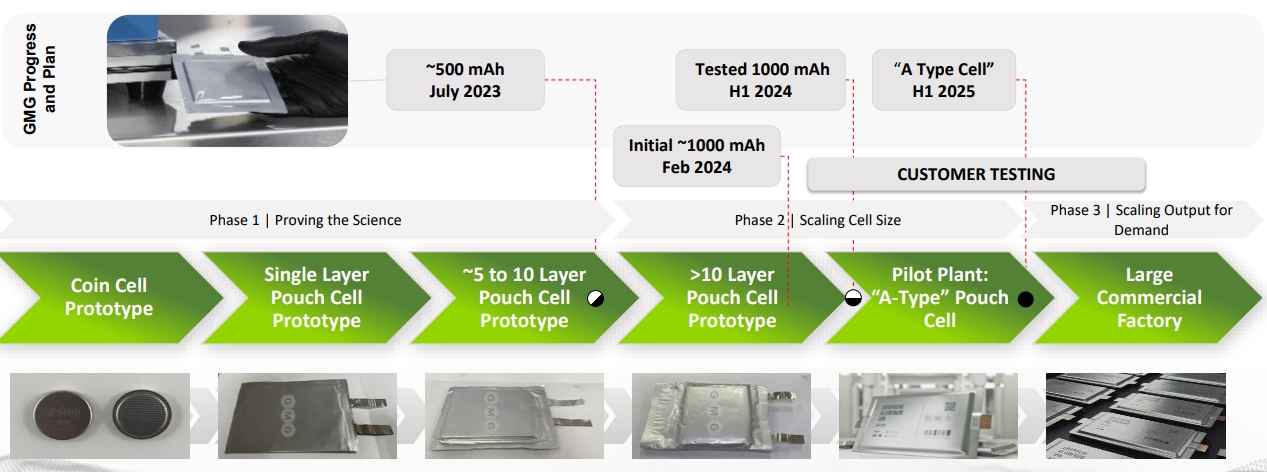
The next step for the company will be its battery technology based on graphene aluminum ion, with a density of 290 Wh/kg, 60x faster charging than lithium-ion batteries, 3x the battery life, and a better fire hazard profile.

Source: GMG
This entry into the battery market might be a big gamble for GMG, but also gives it a unique perspective on the future market that could open for graphene, including in EV and other power-related applications.
